Logic Design for Array-Based Circuits
by Donnamaie E. White
Copyright © 1996, 2001, 2002, 2008, 2016 Donnamaie E. White, WhitePubs Enterprises, Inc.
- Table of Contents
- Preface
- Overview
- Chapter 1 Introduction
- Chapter 2 Structured Design Methodology
- Chapter 3 Sizing the Design
- Chapter 3 Appendix: Case Study in Sizing a Design
- Chapter 4 Design Optimization
- Introduction
- Optimization Approaches
- Design for Speed
- Design to Improve Speed
- Macro options
- Macro functionality
- Example of silicon efficiency
- Alternative implementations
- Internal Net Delays
- Wire-ORs when allowed
- Design to Reduce Internal Cell Utilization
- Design to Reduce I/O Utilization
- Design to Fit the Package
- Example
- Design to Reduce Power
- Design to Reduce Cost
- Basic Design for Circuit Testability
- Basic Design for Circuit Reliability
- Design to Reduce Cost
- Exercises
- Chapter 5 Timing Analysis for Arrays
- Chapter 6 External Set-up and Hold Times
- Chapter 7 Power Considerations
- Case Study: DC Power Computation
- Case Study: AC Power Computation
- Chapter 8 Simulation
- Case Study: Simulation
- Chapter 9 Faults and Fault Detection
- Chapter 10 Design Submission
- ASIC Glossary
Design Optimization
Last Edit July 22, 2001
Basic Design For Circuit Testability
There are several formal methods for design-for-test. These include scan-path and level sensitive scan design. In addition to these, and a part of the design for test requirements, are the follow suggestions for improved circuit testability.
- Become familiar with the macro library BEFORE beginning the macro conversion or design.
- Use synchronous rather than asynchronous circuits whenever possible - functional tests are synchronous.
- Partition the design (use structured design techniques) into smaller,
testable sections, usually along a functional boundary.
In partitioning:- Use degating logic to isolate modules for test.
- Use modular architecture, bus structures.
- Break up long counters (>8).
- Don't bury states.
- Use transparent latches instead of flip/flops where possible.
- Use macros, especially flips/flops and latches, with RESET or SET controls where possible to simplify initialization.
- Avoid feedback loops.
- If unavoidable, provide a means to break up feedback loops during test (degating, enables).
- Avoid redundant logic - minimize! - or add test points to unmask masked faults.
- Avoid derived clocks - they complicate testing.
- Design in test points, especially in sequential logic. Add test points to improve controllability and observability. Perform testability analysis.
- If I/O pins are limited, use demultiplexors to control and multiplexors to observe internal nodes with otherwise poor observability (buried states).
- Any 3-state enable control signal that is internally generated must be externally observable, and should be externally controllable during test.
- Add parity trees for error detection.
- Use Scan Path Design to simplify test sequence generation.
- Use Level Sensitive Scan Design to simplify test sequence generation.
- Use some variation of the Scan Path or LSSD DFT procedures.
- Keep test generation in mind while designing the circuit.
Figure 4-6 Optimization - Circuit Testability
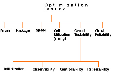
Optimization Issues - Testability
Basic Design For Circuit Reliability
Some specific design suggestions for improved circuit reliability are:
- Become familiar with the macro library BEFORE beginning the macro conversion or design.
- Be aware of "glitch" circuits. Do not use potential glitch circuits to drive clock inputs.
- Avoid one-shot pulse generators.
- Avoid gated and derived clocks.
- Avoid race and hazard conditions. (print on change files can help identify these.) These are generated by having a signal follow two or more paths to a common circuit element (a.k.a. reconvergent fan-out.)
- Avoid feedback loops. If unavoidable, provide a means to break up feedback loops during test (using degating, enables).
- Avoid feedback paths between registers. If present, compute the worst-case set-up and hold times and verify operation. (Feedback from the ECL output macros must be handled with care if used to input to internal latches and flip/flops.)
- Add sufficient GROUND for the number of simultaneously switching outputs and distribute among these outputs (similar to distributed ground in a ribbon cable). Add additional extra ground if there are extra I/O pins available.
- Add extra VCC as needed for the number of simultaneously switching outputs.
- Properly derate fan-out on all distortion-sensitive paths and all clock paths. Keep clock path loading balanced.
- Avoid floating nodes on internal 3-state busses or external bidirectional busses.
- Use Johnson (a.k.a. Mobius, Ring or Twisted-tail) counters or separate flip/flops to decode terminal counts. The loading on the Q outputs is identical, eliminating the loading skew (not the metal skew), and the outputs are a Gray code - only one output changes state per clock cycle. (Binary counter decoding can cause glitches.)
- Compensate for rising and falling edge loading skews and the reversed TTL input translator rising and falling edge skews by inversion as needed to reduce pulse stretch and pulse shrink phenomena.
- Reduce heavy loading on high-speed paths by creating parallel paths with identical macros.
- Use ECL differential inputs and outputs when the frequency exceeds 200-300MHz. The actual frequency boundary will be series-specific.
Figure 4-7 Optimization - Circuit Reliability
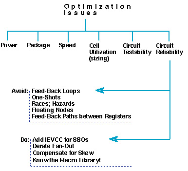
Optimization Issues - Reliability
Copyright © 1996, 2001, 2002, 2008, 2016 Donnamaie E. White , WhitePubs
Enterprises, Inc.
For problems or questions on these pages, contact [email protected]