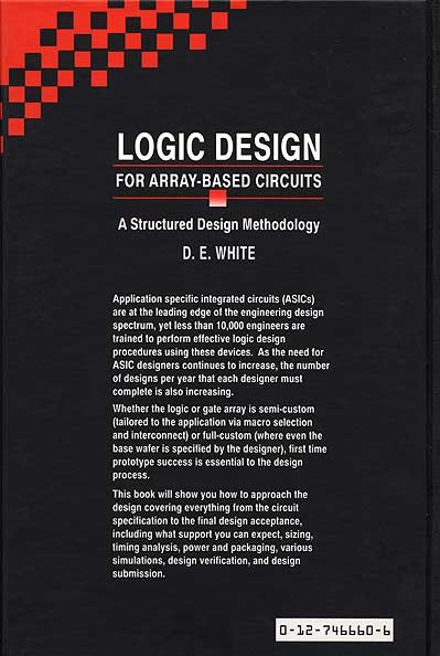
Logic Design for Array-Based Circuits
by Donnamaie E. White
Copyright © 1996, 2001, 2002, 2008, 2016 Donnamaie E. White, WhitePubs Enterprises, Inc.
- Table of Contents
- Preface
- Overview
- Chapter 1 Introduction
- Chapter 2 Structured Design Methodology
- Chapter 3 Sizing the Design
- Chapter 3 Appendix = Case Study in Sizing a Design
- Chapter 4 Design Optimization
- Chapter 5 Timing Analysis for Arrays
- Chapter 6 External Set-up and Hold Times
- Chapter 7 Power Considerations
- Case Study: DC Power Computation
- Case Study: AC Power Computation
- Chapter 8 Simulation
- Case Study: Simulation
- Chapter 9 Faults and Fault Detection
- Chapter 10 Design Submission
- ASIC Glossary
How We Did It
Custom ASIC Design Methodology - 1980-2000 - Pre-RTL - Pre-PrimeTime
- Pre-Synthesis - Pre-edif - Pre-Place & Route
- From Design Criteria to Wafer-Fab
Original Hardcover - Still Available - Amazon.com
And if you are wondering ---
We may have 42+ pieces of software (or classes of software) that we can throw at a design today (2008) and teams that design ASICs that run from 200,000 equivalent gates to 12 million and up equivalent gates. Yes, 12 MILLION! But the overall design flow methodology remains ---- the same. While wafers have run from 3 inches in diameter, to 12 inches (the dinner plate) and are thinking of getting even bigger, the overall design flow remains intact. Every design decision afects the final result. Short-cuts are paid for. Skipping steps will come back and bite you. The design history of many companies, a a fe that no longer exist, isl ittered with bad design flows that attempted to skip over the almost pendatic steps. As one engineering said, after doing it my way, "this works". Surprise, surprise.
Design flow methodology is critical to a first-time silicon success. Everybody's ultimate goal.
Understandting the math and the logic under those steps - Priceless.
Copyright © 1996, 2001, 2002, 2008, 2016 Donnamaie E. White , WhitePubs
Enterprises, Inc.
For problems or questions on these pages, contact [email protected]